The first ASML lithography scanner with a high numerical aperture value (High-NA EUV) was shipped to the needs of Intel back in December last year, its installation was completed at the research center in Oregon by April, and at the last quarterly conference the head of Intel confirmed that the company was preparing receive a second copy of such equipment from ASML.
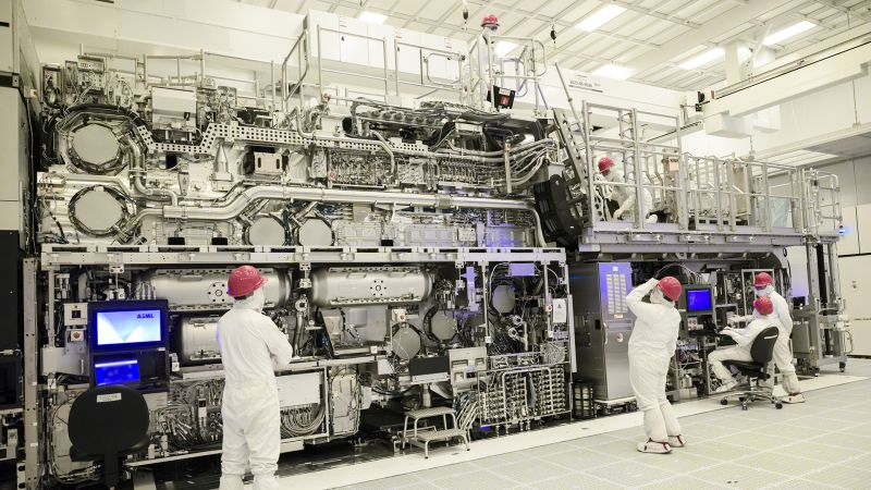
Image Source: Intel
This statement by CEO Patrick Gelsinger, as noted by Reuters, went unnoticed amid the disastrous quarterly report, but this fact was still mentioned from his lips. “The second High-NA tool has been shipped to our Oregon facility,” Intel’s CEO explained succinctly, adding that the company’s early-stage investments in cutting-edge technology are showing good results. As is known, Intel will need such equipment to produce chips using the promising Intel 14A technology from 2027, but at the experimental level it intends to use it as part of the more mature Intel 18A process technology.
In mid-July, representatives of ASML also admitted that the company had begun shipping a second lithography machine for working with High-NA EUV to a certain client, and if we compare this statement with the confessions of the head of Intel, we can understand that we are talking about this company. Intel will have time to receive money for the first lithographic scanner of this class before the end of this year, and the payment for the second may fall as early as next year. Each such lithographic machine costs about 350 million euros.
ASML already has orders for more than a dozen such systems, with clients including Intel, TSMC, Samsung, SK hynix and Micron. At the same time, TSMC claims that it will not need such scanners to produce chips using A16 technology, but it still does not refuse experiments with such equipment. The memory manufacturers listed above expect to begin using high numerical aperture EUV lithographs from 2025 to 2026.