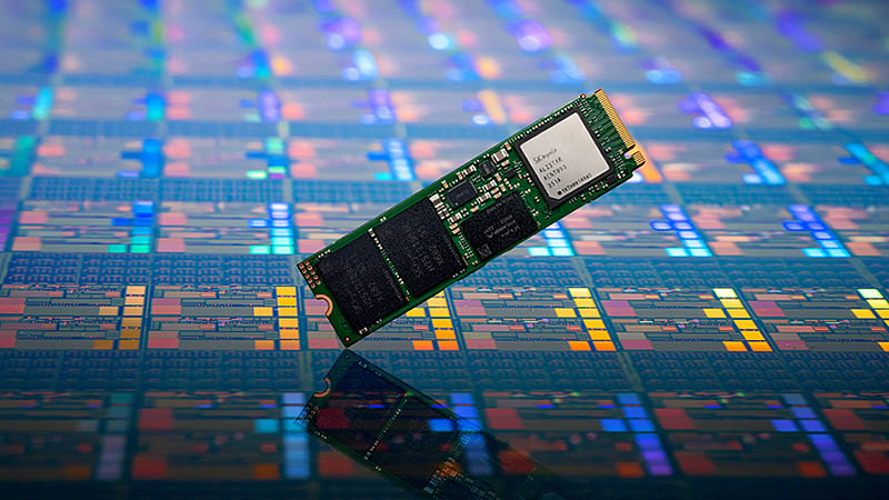
As the battle for leadership in the HBM space intensifies, competition in the NAND market also intensifies. SK hynix has begun developing 400-layer NAND flash memory to provide higher storage densities, with plans to launch the technology into mass production by the end of 2025.

Image Source: SK Hynix
According to the analytical publication TrendForce, citing a report from the Korean publication etnews, SK hynix is currently already collaborating with partners and equipment suppliers whose connections are necessary to develop technological processes for the production of NAND with more than 400 layers using hybrid wafer-wafer technology. to-plate” (W2W). Increasing the number of layers should improve the performance and energy efficiency of NAND memory, which, according to experts, will have a positive effect on the characteristics of devices using it.
Previously, the company used the Peripheral Under Cell (PUC) method and placed the control logic under the NAND cells, but as the number of layers increased, problems arose with damage to the peripheral circuits due to high heat and pressure. The new method involves manufacturing cells and control circuits on separate wafers and then connecting them, which should lead to a problem-free increase in the number of NAND layers.
But not only SK hynix is engaged in research and development in the field of increasing the number of NAND memory layers. Samsung previously confirmed that it has begun mass production of 1-terabyte triple-layer cell (TLC) 9th generation NAND (V-NAND), with the number of layers reaching 290, setting a goal of increasing the number of V-NAND layers to 1000 by 2030. In turn, the American company Micron Technology announced the client SSD 2650, which became the first product built on 276-level 3D NAND. And Japanese memory chip manufacturer Kioxia, after successfully increasing the number of 3D NAND levels to 218 in 2023, announced the possibility of reaching 1000 levels by 2027.