Enthusiasts have published a detailed image of the 4nm die of the new AMD Strix Point mobile processor (Ryzen AI 300), on which all components of the chip are clearly visible. Along with the image was a detailed description of what components were contained in the chip.
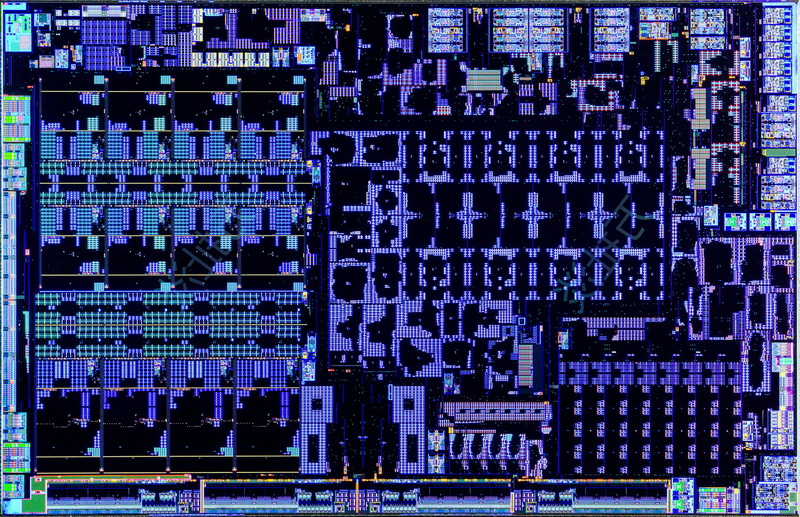
Image source: Bilibili
The new Strix Point is significantly larger than the Phoenix crystal – its dimensions are 12.06 × 18.71 mm versus 9.06 × 15.01 mm for the previous generation chip. The increase in area is mainly due to the fact that Strix Point received larger CPU, iGPU and NPU units. In addition, AMD transferred the die of the new chip from the TSMC N4 process technology (Phoenix and its successor Hawk Point) to the improved TSMC N4P process technology.
The new processor has 12 computing cores, divided into two CCX blocks, one of which contains four Zen 5 cores and 16 MB of L3 cache, and the second contains eight energy-efficient Zen 5c cores and 8 MB of L3 cache dedicated to them. The CCX blocks are connected to the rest of the processor via an Infinity Fabric bus. A very large iGPU unit occupies the central part of the chip. It is based on the RDNA 3.5 graphics architecture and contains eight workgroup processors (WGP) or 16 execution units (CU), which include 1024 stream processors. Other key components of the iGPU include four rendering units with 16 ROPs and control logic. The integrated Strix Point graphics has its own 2 MB of L2 cache.
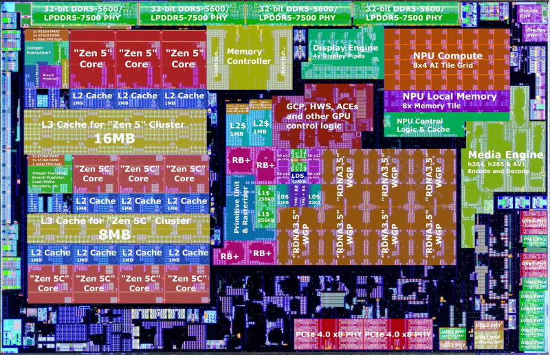
Image source: X / @GPUsAreMagic
Next to the iGPU, on the right side of the Strix Point die, are its sister components, the Media Engine and Display Engine. The former provides hardware acceleration for encoding and decoding of h.264, h.265 and AV1, as well as several legacy video formats. The Display Engine is responsible for encoding the iGPU’s output frame into various connector formats (such as DisplayPort, eDP, HDMI), including hardware-accelerated stream compression (DSC). Display PHY circuits are responsible for the physical layer of connecting the iGPU to the video connectors.
The NPU is the third key logical component of the Strix Point. The new AMD processors use the second generation of NPUs, whose physical dimensions have become noticeably larger than those of Phoenix. The new NPU is based on the advanced XDNA 2 architecture and contains 32 AI engine tiles that interact with its own high-speed local memory and control logic, which in turn is connected to the Infinity Fabric bus. This NPU is designed to meet Microsoft’s Copilot Plus PC ecosystem requirements and delivers 50 TOPS (trillion operations per second) performance.
The memory controller in Strix Point supports dual-channel (160-bit) DDR5-5600 and 128-bit LPDDR5 RAM with speeds up to 7500 MT/s. The controller has an unspecified SRAM cache size, which is noted to have also been seen in Phoenix 2 and Phoenix dies.
The Strix Point die has a smaller PCIe root complex than the Phoenix, which in turn is smaller than the Cezanne die (Ryzen 5000). Over the past three generations of processors, AMD has reduced the number of PCIe lanes by four. If Cezanne has 24 PCIe 3.0 lanes (x16 for video card + x4 for NVMe SSD + x4 for chipset bus or GPP), then Phoenix has the number of lanes reduced to 20 PCIe 4.0 (x8 for video card + x4 for NVMe SSD + x4 for chipset bus or GPP+x4 for USB4). And the new Strix Point has the number of PCIe 4.0 lanes reduced to 16 (x8 for the video card + x4 for NVMe SSD + x4 for USB4 or GPP).
The reduction in the number of PCIe lanes is due to the fact that Strix Point is designed to compete with Intel Lunar Lake, which also only has four PCIe lanes per graphics card or GPP. With the release of Intel’s Arrow Lake-H and Arrow Lake-HX processors, AMD is expected to release Fire Range chips that will feature 28 PCIe 5.0 lanes and can be paired with even the fastest discrete mobile GPUs.