Manufacturers of semiconductor components use so-called EUV lithography only at certain stages of the technological process, their number is increasing from generation to generation. So, if Samsung was limited to 20 EUV layers when producing 3nm chips, then after switching to a 2nm process technology their number will increase by 30%.
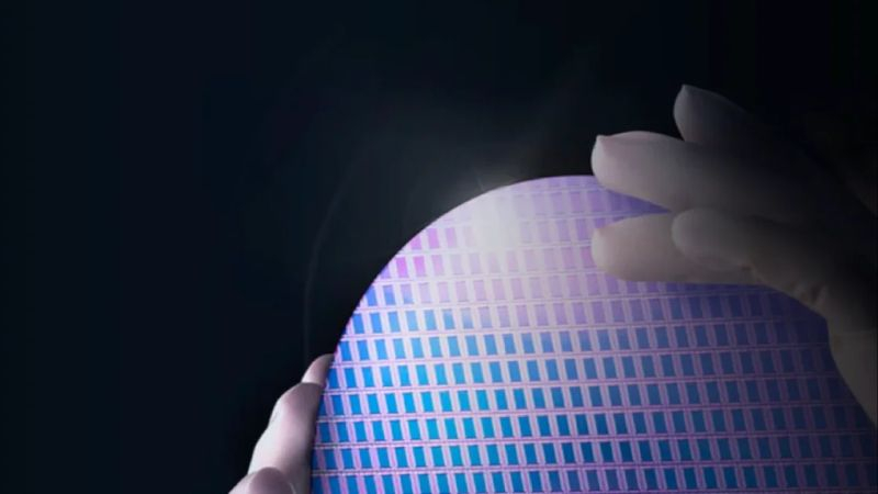
Image Source: Samsung Electronics
The South Korean publication The Elec reported this last week, citing its own sources. In other words, with 2nm technology, Samsung will use ultra-hard ultraviolet lithography to process approximately 27 layers. For comparison, TSMC processes 25 layers using EUV lithography when producing chips using the N3 process technology. According to Korean sources, after switching to the production of 1.4-nm chips in 2027, Samsung expects to process more than 30 layers using the EUV method.
Accordingly, all these plans imply that Samsung will need more lithography scanners, as well as related equipment designed to work with EUV lithography. The largest supplier of such equipment, the Netherlands’ ASML, intends to ship about 70 corresponding scanners to customers over the next two years, each of which costs more than $100 million. The need for chip manufacturers in capital expenditures will increase after the transition to equipment with a high numerical aperture (High-NA), since the corresponding scanner will cost $300 million. The most active buyer of these scanners will be Intel, but TSMC is in no hurry to introduce this technology precisely for economic reasons.